Visualizing Semiconductor Success: A Comprehensive Guide to Python Wafer Map Plots
Related Articles: Visualizing Semiconductor Success: A Comprehensive Guide to Python Wafer Map Plots
Introduction
With enthusiasm, let’s navigate through the intriguing topic related to Visualizing Semiconductor Success: A Comprehensive Guide to Python Wafer Map Plots. Let’s weave interesting information and offer fresh perspectives to the readers.
Table of Content
- 1 Related Articles: Visualizing Semiconductor Success: A Comprehensive Guide to Python Wafer Map Plots
- 2 Introduction
- 3 Visualizing Semiconductor Success: A Comprehensive Guide to Python Wafer Map Plots
- 3.1 The Importance of Wafer Map Visualization
- 3.2 Python Libraries for Wafer Map Plotting
- 3.3 Creating a Wafer Map Plot in Python
- 3.4 Enhancing Wafer Map Plots with Advanced Features
- 3.5 FAQs Regarding Python Wafer Map Plots
- 3.6 Tips for Effective Wafer Map Plotting in Python
- 3.7 Conclusion
- 4 Closure
Visualizing Semiconductor Success: A Comprehensive Guide to Python Wafer Map Plots
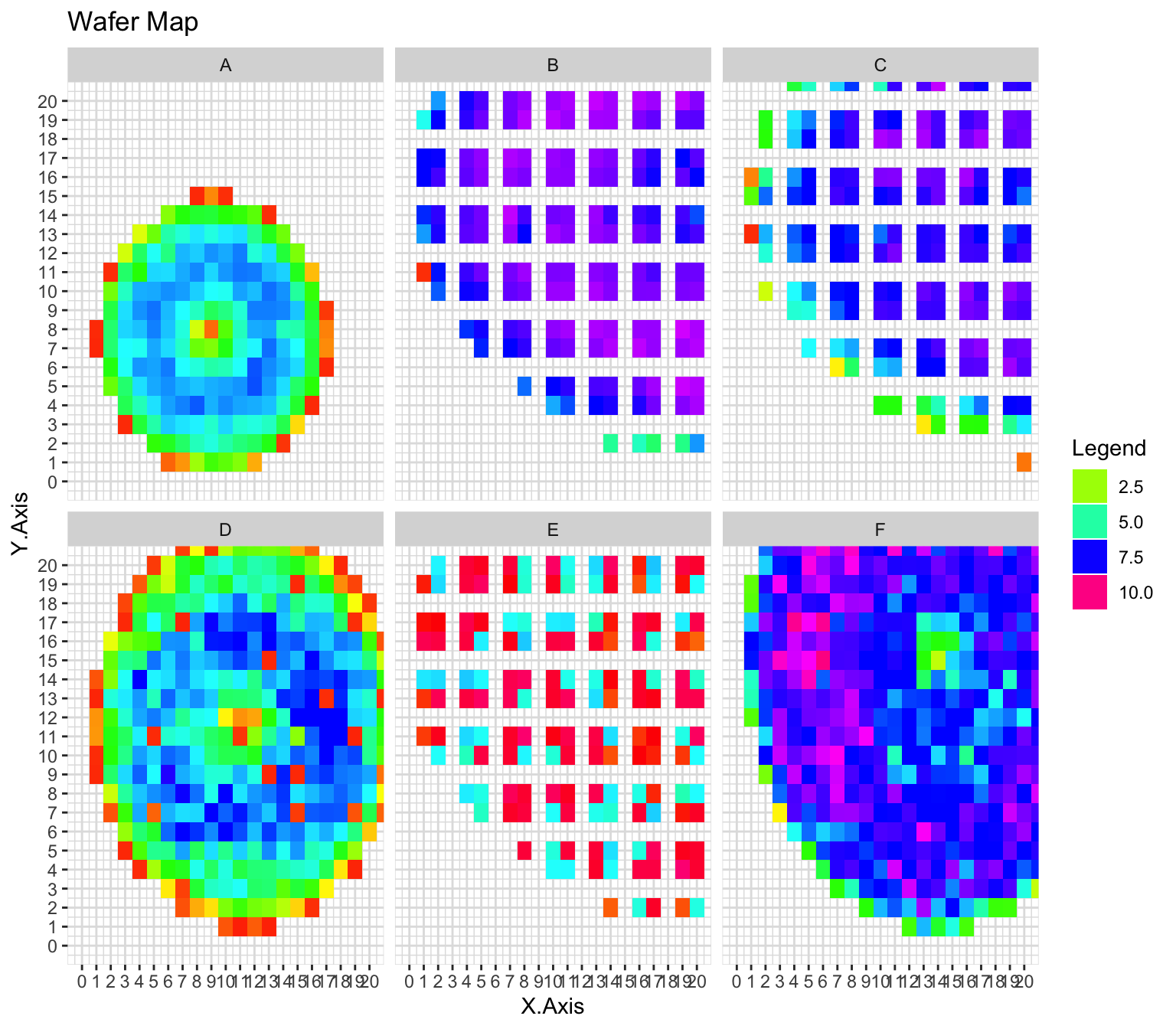
In the realm of semiconductor manufacturing, the wafer map stands as a crucial visual representation of the health and performance of a production run. Each wafer, a thin slice of silicon, contains hundreds or even thousands of individual semiconductor devices. A wafer map visually displays the yield, defects, and overall quality of these devices across the wafer’s surface. Understanding the patterns and trends within a wafer map is essential for optimizing manufacturing processes, identifying potential issues, and ensuring the consistent production of high-quality chips.
Python, with its versatile libraries and open-source nature, has become a powerful tool for creating insightful and informative wafer map plots. This article delves into the intricacies of Python wafer map plotting, providing a comprehensive guide for semiconductor professionals seeking to leverage this powerful visualization technique.
The Importance of Wafer Map Visualization
Wafer map visualization plays a pivotal role in semiconductor manufacturing, offering numerous benefits:
- Process Monitoring and Control: By analyzing the spatial distribution of defects and yield across the wafer, engineers can identify potential issues in the manufacturing process, such as equipment malfunctions, contamination, or process variations. This allows for timely adjustments and optimization of production parameters to ensure consistent high-quality output.
- Defect Analysis and Root Cause Identification: Wafer maps provide a visual representation of defect locations, enabling engineers to identify patterns and correlations between defects and specific process steps. This information is crucial for pinpointing the root cause of defects and implementing corrective actions.
- Yield Improvement and Cost Reduction: By identifying and addressing process issues early on, wafer map analysis helps improve overall yield and reduce manufacturing costs. This is achieved by minimizing the number of defective devices and maximizing the number of functional chips produced per wafer.
- Data-Driven Decision Making: Wafer map visualization facilitates data-driven decision making by providing a clear and concise visual summary of production performance. This enables engineers and managers to make informed decisions regarding process adjustments, equipment maintenance, and resource allocation.
Python Libraries for Wafer Map Plotting
Python boasts a rich ecosystem of libraries specifically designed for data visualization, making it an ideal choice for creating informative wafer map plots. Here are some of the most popular and effective libraries:
- Matplotlib: The cornerstone of Python plotting, Matplotlib provides a flexible and powerful framework for creating static, interactive, and animated visualizations. Its intuitive syntax and extensive customization options make it well-suited for creating basic and advanced wafer map plots.
- Seaborn: Building upon Matplotlib, Seaborn offers a higher-level interface for creating visually appealing and statistically informative plots. Its built-in functions simplify the process of creating aesthetically pleasing wafer maps with enhanced statistical insights.
- Plotly: For interactive and web-based visualizations, Plotly is a powerful library that allows for creating dynamic wafer maps with zoom, pan, and hover features. Its ability to integrate with web applications and dashboards makes it ideal for real-time monitoring and data exploration.
- Bokeh: Similar to Plotly, Bokeh specializes in interactive and web-based visualizations. It offers a flexible and customizable framework for creating interactive wafer maps with advanced features like data filtering, tooltips, and custom annotations.
Creating a Wafer Map Plot in Python
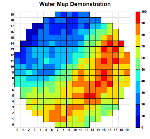
To illustrate the process of creating a wafer map plot in Python, let’s consider a simple example using Matplotlib. Assume we have a dataset containing the yield data for each die on a wafer, represented as a 2D array.
import matplotlib.pyplot as plt

# Sample wafer yield data
wafer_yield = [[0.9, 0.8, 0.7, 0.6],
                [0.8, 0.9, 0.8, 0.7],
                [0.7, 0.8, 0.9, 0.8],
                [0.6, 0.7, 0.8, 0.9]]

# Create a figure and axes object
fig, ax = plt.subplots()

# Plot the wafer yield data as a heatmap
heatmap = ax.imshow(wafer_yield, cmap="viridis", interpolation="nearest")

# Set axis labels and title
ax.set_xlabel("Die Column")
ax.set_ylabel("Die Row")
ax.set_title("Wafer Yield Map")

# Add a colorbar to the plot
plt.colorbar(heatmap, label="Yield")

# Show the plot
plt.show()
This code snippet demonstrates the basic steps involved in creating a wafer map plot using Matplotlib:
-
Import necessary libraries: Import the
matplotlib.pyplotlibrary for plotting functionalities. - Define wafer data: Create a 2D array representing the wafer yield data, with each element representing the yield of a specific die.
-
Create figure and axes: Use
plt.subplots()to create a figure and axes object for the plot. -
Plot heatmap: Use
ax.imshow()to plot the wafer yield data as a heatmap, specifying the colormap and interpolation method. - Set labels and title: Add labels to the axes and a descriptive title to the plot.
- Add colorbar: Include a colorbar to indicate the mapping between color values and yield values.
-
Display the plot: Use
plt.show()to display the generated wafer map plot.
Enhancing Wafer Map Plots with Advanced Features
Python libraries offer a wide range of customization options for enhancing wafer map plots and conveying complex information effectively:
- Colormaps: Select appropriate colormaps to visually represent the data distribution. For example, a diverging colormap can highlight both high and low yield areas, while a sequential colormap can represent gradual changes in yield.
- Annotations: Add annotations to the plot to highlight specific regions of interest, such as defect locations, process variations, or outlier dies. Annotations can include text labels, markers, or custom shapes.
- Interactive Features: Leverage interactive plotting libraries like Plotly or Bokeh to create dynamic wafer maps with zoom, pan, and hover functionalities. This allows for detailed exploration of the data and identification of subtle patterns.
- Statistical Analysis: Integrate statistical analysis techniques into the plotting process to display additional insights, such as mean yield, standard deviation, and statistical significance of observed patterns.
- Data Filtering and Grouping: Apply data filtering and grouping techniques to create multiple wafer maps, visualizing different subsets of the data based on specific criteria, such as process parameters, wafer lots, or defect types.
- Custom Legends: Create custom legends to explain the meaning of different colors, markers, or annotations used in the plot. This ensures clear and concise interpretation of the visualized data.
FAQs Regarding Python Wafer Map Plots
1. What are the different types of wafer map plots?
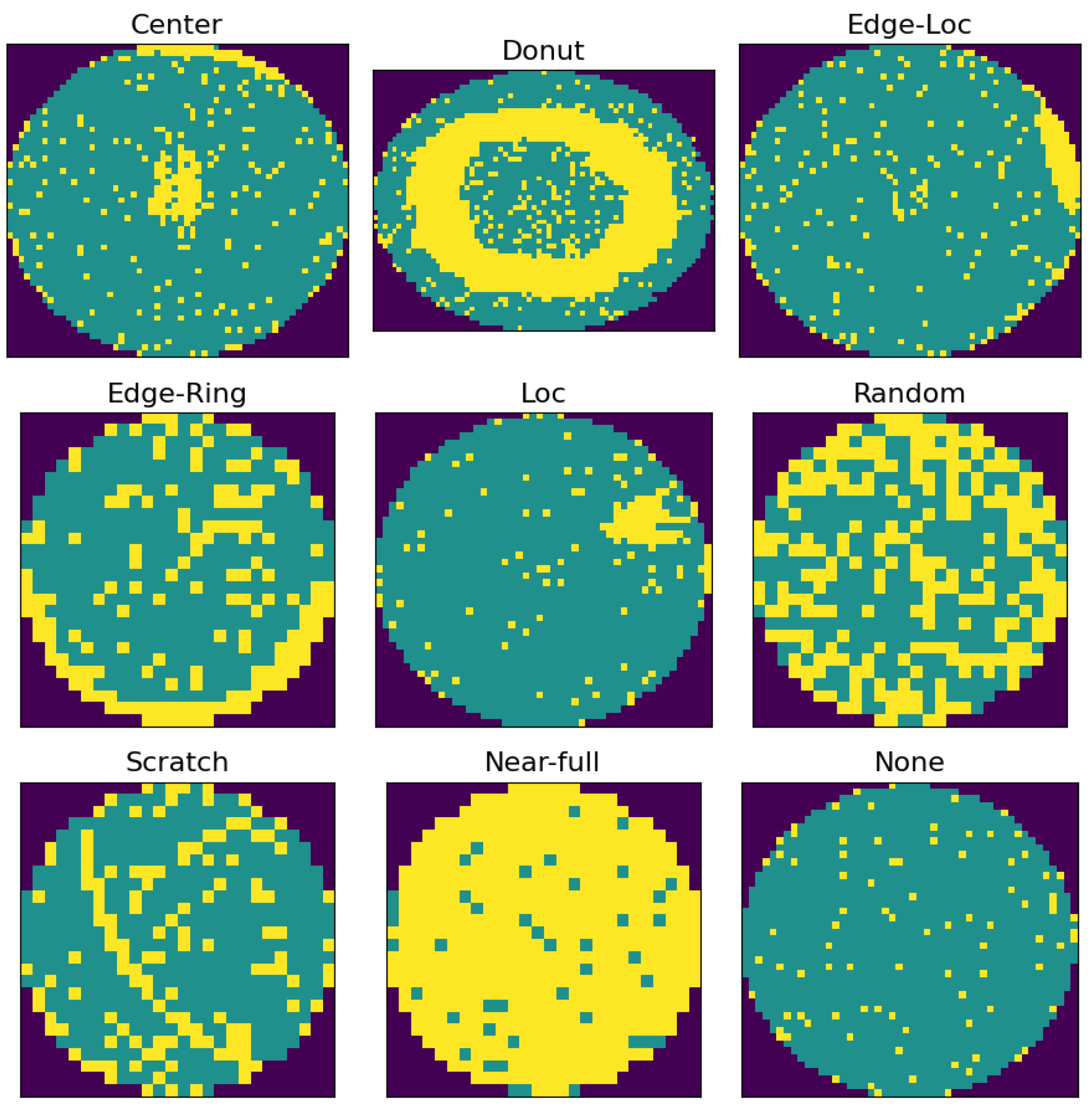
Wafer map plots can be classified based on the type of data they represent:
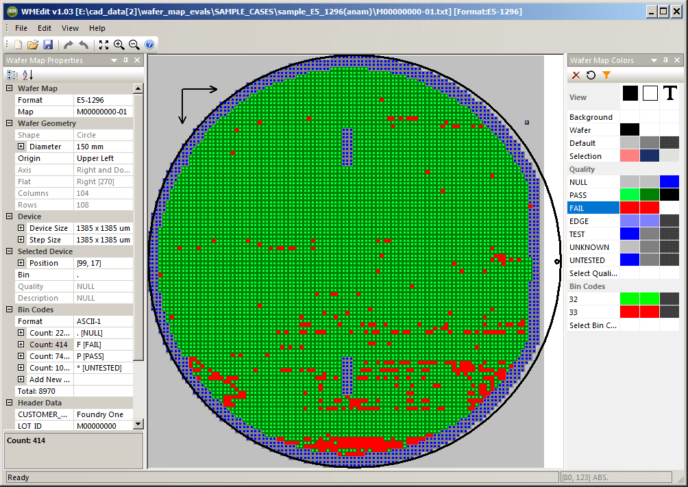
- Yield Maps: Visualize the yield of each die on the wafer, typically represented as a heatmap.
- Defect Maps: Show the location and type of defects detected on the wafer, often represented using different colors or markers for each defect type.
- Process Parameter Maps: Display the variation of process parameters across the wafer, such as temperature, pressure, or exposure time.
- Combined Maps: Combine different data types on the same map, such as yield and defect location, to provide a comprehensive view of the wafer’s performance.
2. How can I incorporate real-time data into a wafer map plot?
Libraries like Plotly and Bokeh allow for real-time data visualization, enabling the creation of dynamic wafer maps that update as new data becomes available. This is particularly useful for monitoring production processes and identifying issues in real-time.
3. What are some best practices for creating effective wafer map plots?
- Choose appropriate colormaps and scales: Select colormaps that effectively represent the data distribution and ensure a clear visual distinction between different data values.
- Use clear and concise labels and annotations: Provide informative labels for axes, legends, and annotations to ensure easy interpretation of the plot.
- Optimize plot size and resolution: Choose an appropriate plot size and resolution to ensure readability and visual clarity.
- Consider the target audience: Tailor the plot’s complexity and level of detail to the knowledge and experience of the intended audience.
Tips for Effective Wafer Map Plotting in Python
- Start with a clear objective: Define the specific insights you want to gain from the wafer map plot before starting the visualization process.
- Clean and preprocess the data: Ensure the data is accurate, consistent, and properly formatted before creating the plot.
- Experiment with different plotting libraries and techniques: Explore different libraries and plotting techniques to find the most effective way to visualize your data.
- Iterate and refine the plot: Don’t settle for the first draft. Continuously refine the plot based on feedback and insights gained from the visualization process.
- Document your code and analysis: Create clear and concise documentation for your code and analysis, ensuring reproducibility and ease of sharing with others.
Conclusion
Python wafer map plots offer a powerful and versatile tool for visualizing and analyzing semiconductor manufacturing data. By leveraging the capabilities of Python libraries like Matplotlib, Seaborn, Plotly, and Bokeh, semiconductor professionals can create insightful and informative plots that aid in process monitoring, defect analysis, yield improvement, and data-driven decision making. This comprehensive guide provides a solid foundation for creating effective wafer map plots, enabling users to unlock the full potential of this visualization technique and drive continuous improvement in semiconductor manufacturing.


Closure
Thus, we hope this article has provided valuable insights into Visualizing Semiconductor Success: A Comprehensive Guide to Python Wafer Map Plots. We thank you for taking the time to read this article. See you in our next article!