Navigating the Semiconductor Landscape: A Deep Dive into Wafer Map Python
Related Articles: Navigating the Semiconductor Landscape: A Deep Dive into Wafer Map Python
Introduction
With great pleasure, we will explore the intriguing topic related to Navigating the Semiconductor Landscape: A Deep Dive into Wafer Map Python. Let’s weave interesting information and offer fresh perspectives to the readers.
Table of Content
Navigating the Semiconductor Landscape: A Deep Dive into Wafer Map Python

The semiconductor industry, a cornerstone of modern technology, relies on intricate processes to manufacture microscopic components that power our devices. At the heart of this manufacturing lies the wafer, a thin slice of silicon that serves as the foundation for integrated circuits. Visualizing and analyzing data from these wafers is crucial for understanding production yields, identifying defects, and optimizing manufacturing processes. This is where the power of Python, coupled with its diverse libraries, shines.
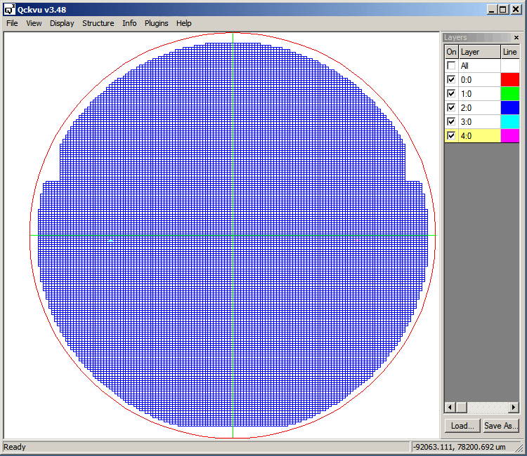
Understanding Wafer Maps
A wafer map is a visual representation of the individual dies (functional units) on a silicon wafer. It provides a comprehensive overview of the wafer’s health, highlighting critical information such as:
- Die Locations: The exact position of each die on the wafer.
- Die Status: Whether a die is functional, defective, or partially functional.
- Defect Types: The nature of any defects found on the die, such as scratches, cracks, or contamination.
- Measurement Data: Measurements related to die performance, such as electrical characteristics or dimensions.
Wafer maps are crucial for:
- Yield Analysis: Determining the percentage of functional dies on a wafer, a key metric for assessing production efficiency.
- Defect Analysis: Identifying patterns in defect locations and types, enabling engineers to pinpoint root causes and implement corrective actions.
- Process Optimization: Analyzing wafer map data to identify areas where process parameters can be adjusted to improve yield and reduce defects.
- Quality Control: Monitoring wafer map data to ensure consistent quality throughout the manufacturing process.
Python: A Powerful Tool for Wafer Map Analysis
Python, with its versatility and extensive libraries, has become the go-to language for wafer map analysis. Its ability to handle complex data structures, perform advanced calculations, and generate informative visualizations makes it an ideal tool for this task.
Essential Python Libraries for Wafer Map Analysis
Several Python libraries play a vital role in wafer map analysis:
- NumPy: A fundamental library for numerical computing, providing tools for array manipulation, mathematical operations, and data analysis.
- Pandas: A powerful data manipulation and analysis library that allows for efficient data loading, cleaning, transformation, and analysis.
- Matplotlib: A comprehensive plotting library for creating static, interactive, and animated visualizations, enabling clear representation of wafer map data.
- Seaborn: A statistical data visualization library that simplifies the creation of informative and aesthetically pleasing plots for wafer map analysis.
- Scikit-learn: A machine learning library that provides tools for building predictive models to identify potential defects or predict yield based on wafer map data.
- PyQt: A cross-platform graphical user interface (GUI) library that allows for the development of custom applications for interactive wafer map visualization and analysis.
Illustrative Example: Analyzing Wafer Map Data with Python
Consider a scenario where we have a CSV file containing wafer map data. Each row represents a die, and columns contain information such as die location, status, and defect type.
Code Snippet:
import pandas as pd
import matplotlib.pyplot as plt

# Load wafer map data from CSV file
wafer_map = pd.read_csv('wafer_map.csv')

# Filter for defective dies
defective_dies = wafer_map[wafer_map['Status'] == 'Defective']

# Create a scatter plot of defective die locations
plt.scatter(defective_dies['X_Coord'], defective_dies['Y_Coord'], c='red', marker='x')
plt.title('Defective Die Locations on Wafer')
plt.xlabel('X Coordinate')
plt.ylabel('Y Coordinate')
plt.show()

# Calculate yield
yield_percentage = len(wafer_map[wafer_map['Status'] == 'Functional']) / len(wafer_map) * 100
print(f'Wafer Yield: yield_percentage:.2f%')
This code snippet demonstrates basic data loading, filtering, visualization, and yield calculation using Python libraries. It provides a starting point for more complex analyses, such as identifying defect clusters, analyzing trends over time, or developing predictive models.
Benefits of Using Python for Wafer Map Analysis
- Enhanced Efficiency: Python’s automation capabilities streamline data processing and analysis tasks, saving time and effort compared to manual methods.
- Increased Accuracy: Python’s robust libraries and data structures minimize errors and ensure accurate analysis results.
- Improved Visualization: Python’s visualization libraries provide powerful tools for creating clear and informative representations of wafer map data, enabling better communication and understanding.
- Advanced Analytics: Python’s machine learning capabilities enable the development of predictive models for defect detection, yield prediction, and process optimization.
- Flexibility and Customization: Python’s open-source nature and vast community support allow for customization and adaptation to specific requirements and workflows.
FAQs about Wafer Map Python
1. What are the common data formats used for wafer maps?
Wafer map data is often stored in CSV (Comma Separated Values), Excel, or proprietary formats. Python libraries like Pandas can read and manipulate data from various sources.
2. How can I visualize wafer map data in 3D?
Libraries like Matplotlib and Plotly can be used to create 3D visualizations of wafer maps, providing a more comprehensive understanding of defect distribution and spatial relationships.
3. What are some advanced techniques for analyzing wafer map data?
Advanced techniques include clustering algorithms for identifying defect clusters, statistical process control (SPC) for monitoring process variations, and machine learning models for predicting defects and yield.
4. How can I integrate wafer map analysis with other manufacturing data?
Python allows for data integration from various sources, such as process control systems, sensor readings, and other databases. This integration enables comprehensive analysis of wafer data within the broader manufacturing context.
5. Are there any pre-built Python tools specifically designed for wafer map analysis?
While no dedicated tools exist, several open-source libraries and code repositories offer specialized functions and workflows for wafer map analysis, providing a starting point for customized solutions.
Tips for Effective Wafer Map Python Analysis
- Clearly define your objectives: Before starting analysis, clearly identify the specific questions you want to answer and the insights you aim to gain from the data.
- Data cleaning and preparation: Ensure the data is clean, consistent, and ready for analysis. This may involve handling missing values, correcting errors, and standardizing data formats.
- Visualize the data: Create informative visualizations to gain a clear understanding of the data patterns and trends.
- Experiment with different analysis techniques: Explore various statistical methods, machine learning algorithms, and visualization tools to uncover hidden insights.
- Document your code and analysis: Maintain clear documentation to track your analysis process, ensure reproducibility, and facilitate collaboration.
Conclusion
Python has emerged as a powerful and versatile tool for wafer map analysis in the semiconductor industry. Its ability to handle complex data, perform advanced calculations, and generate insightful visualizations makes it an indispensable asset for understanding wafer health, optimizing production processes, and improving overall manufacturing efficiency. As the semiconductor industry continues to innovate and push the boundaries of miniaturization, the role of Python in wafer map analysis will only become more critical, enabling engineers to navigate the intricacies of this complex and vital field.


![[PDF] Anomaly Detection and Segmentation for Wafer Defect Patterns Using Deep Convolutional](https://d3i71xaburhd42.cloudfront.net/9221ae991591154a94b416fa4812e991d06ea5a5/6-Figure12-1.png)


Closure
Thus, we hope this article has provided valuable insights into Navigating the Semiconductor Landscape: A Deep Dive into Wafer Map Python. We appreciate your attention to our article. See you in our next article!